Inside the 6502
A complete, transistor-level reverse engineering of the MOS 6502 microprocessor — from a decapped chip and a microscope to a full schematic. Originally published in Hungarian in 2001, now translated to English.
The 6502 was one of the processors that kick-started the microcomputer revolution. Its first major application was the Apple II; in Hungary most people got to know it through the Commodore machines.
It was made in a 6 µm nMOS process with depletion-load gates, a single layer of aluminium metallization, and roughly 3,900 transistors. The plastic package can be removed with, for example, hot concentrated sulfuric acid; after rinsing, the die can be examined well under an optical microscope.
Decoding it took several months of work. The schematic is complete, though it may still contain mistakes.
- 6 µmnMOS process
- ~3,900transistors
- 1metal layer
- 56 / 13instructions / addressing modes
Explore
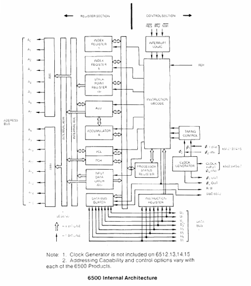
Architecture
The 65xx family has a minimal set of registers, but thanks to its many addressing modes they can be used very efficiently: a 16-bit program counter, an 8-bit stack pointer, the status (flag) register, the accumulator, and the X and Y index registers. Stack operations and instructions working on the lowest 256 bytes of memory (the zero page) are one clock cycle faster than the rest, which speed-optimised software exploits. Simple instructions finish in 2–3 cycles. BCD arithmetic is supported automatically once the D flag is set — no separate adjust instruction and no extra clock cycle are needed.
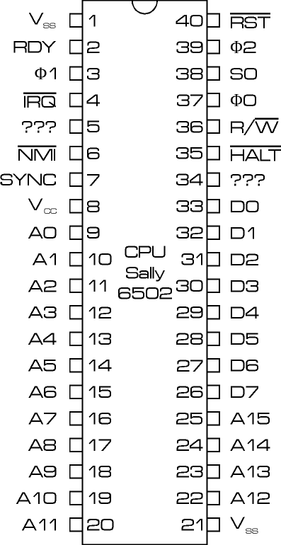
Pinout
Downloads
- Full die image (PNG, 3634 × 5698)19.8 MB
- Full schematic, one vector sheet (PDF)0.4 MB
- Printable schematic, A3 pages (PostScript)6.4 MB
- Printable schematic, A4 pages (PostScript)10.7 MB
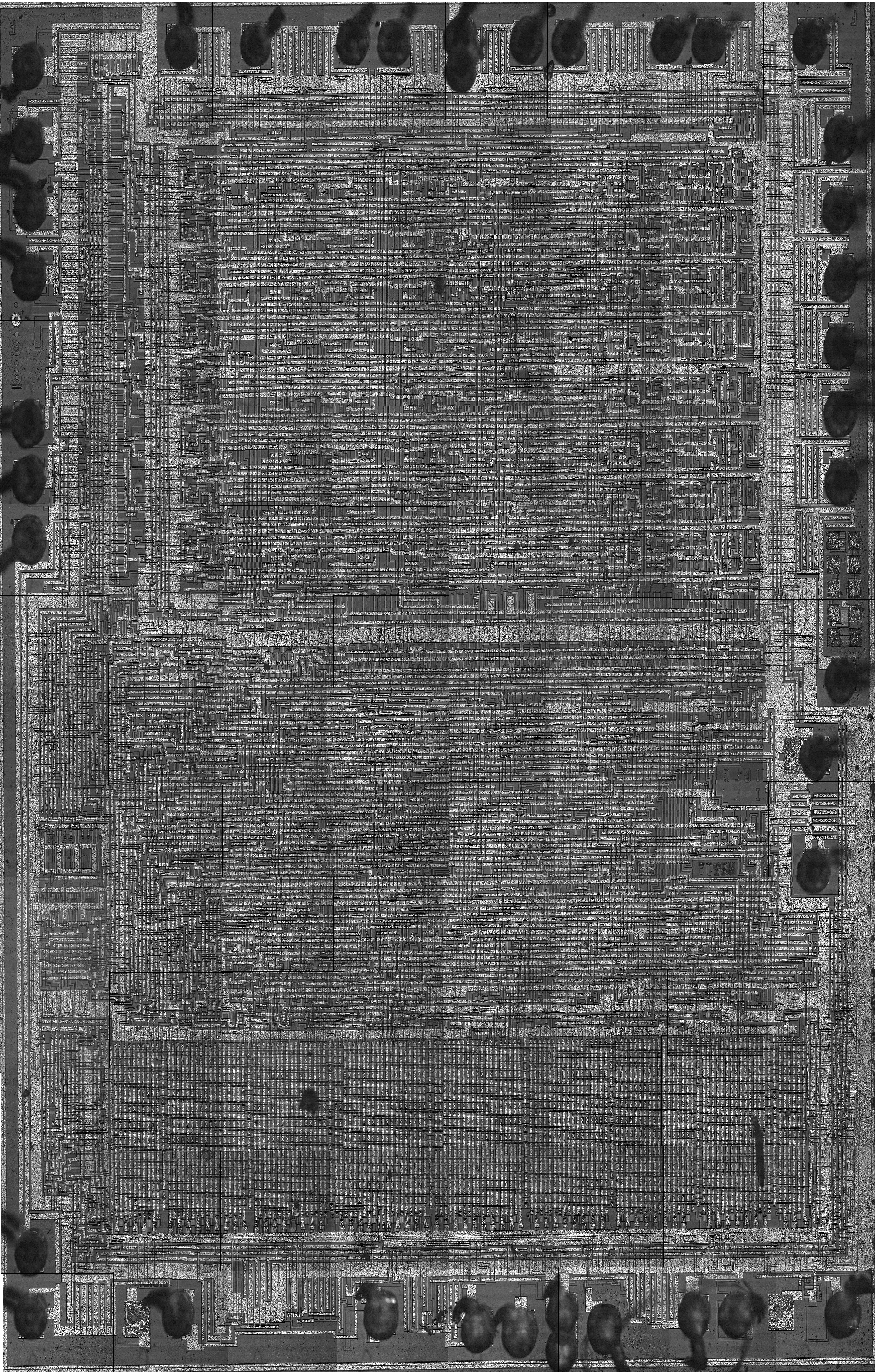
The layout is protected by copyright and must not be used directly for manufacturing. Looking at it, decoding it and taking ideas from it is fine, and everything published here can be downloaded freely. Comments and any errors you find are welcome at [email protected]