How the circuits work
Circuits from every part of the block diagram, with descriptions of how they work and, for illustration, the matching pieces of the layout.
Clock generator
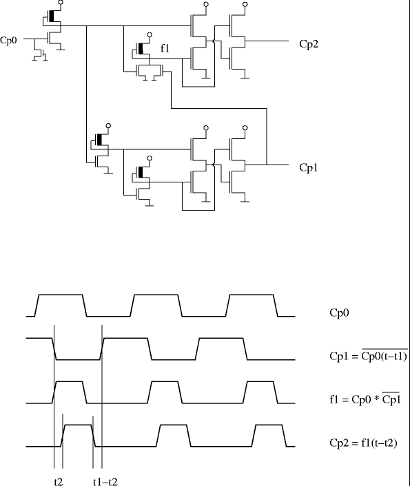
From the Φ0 clock input (980 kHz, labelled Cp0 on the schematics) the processor generates its own two phase signals, Cp1 and Cp2. They never overlap, so they divide every clock cycle sharply into two time slices. This is useful not only for writing the registers — external devices may need it as well, so both phases are brought out to pins.
The trick of the clock generator is that two push-pull inverter pairs, which deliver large currents (the phase signals have to reach every corner of the chip) and are slow, double as delay elements that shift the signals in time, as the figure below shows. The circuit itself is very simple and uses few transistors, but it occupies a lot of silicon area, just like the bus drivers.
Instruction decoder
Its core is the PLA, built from NOR gates, which takes its inputs from the instruction register and the timing generator. Its outputs drive the register block directly.
Another important job is finding instruction boundaries. These are needed to issue the fetch signal, to drive the SYNC pin, and for the interrupt logic (interrupts are taken only at instruction boundaries). When the next opcode has to be fetched depends on the previous opcode, because most instructions take a fixed number of clock cycles, whether or not there is BCD correction. The exceptions are conditional branches: depending on whether the condition holds, either a jump or a fetch follows.
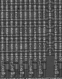
On the layout the columns are the outputs of the NOR gates, and the rows are the true and complemented inputs. The arrangement is quite clever, because a single contact can carry two bits of information: the complemented input of one row and the true input of the row below it.
The 8 data-bit inputs are not in order but scrambled. Some columns are not contacted anywhere — for example one that does not belong to the decoder at all, but carries the IRQ request.
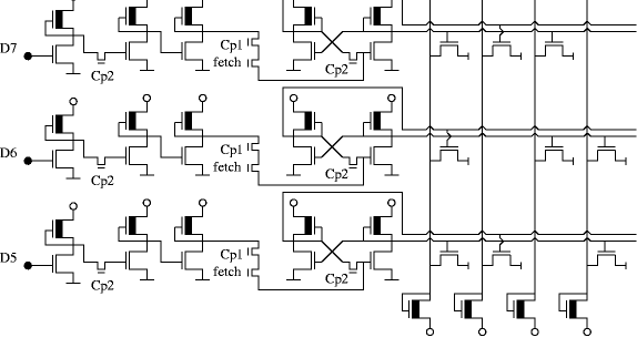
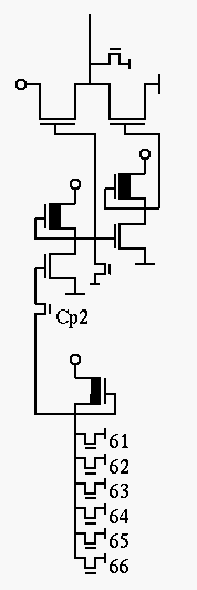
The PLA outputs feed a combinational network that also uses quite a few internal control signals, such as the internal Ready signal, Sync, and one of the timing generator outputs. Passing through complex gates, the PLA outputs reach push-pull inverters, which drive a long polysilicon line and 8 transfer gates. These directly control reading and writing of the registers, the operation of the ALU, and the bus drivers, address and data lines.
The figure on the left shows a simple case: the control for writing the accumulator. PLA outputs 61 to 66 gate the following operations: writing X or Y to A, logical operations, addition/subtraction, shifting the accumulator, and loading it from the stack.
There are much more complicated circuits that also control the transfer gates of the register block, for example deciding when to copy one internal bus onto another, or where the ALU takes its inputs from.
Undocumented ("illegal") opcodes
Gates with many inputs process those PLA outputs that are not fully specified: some bits of the opcode are tied neither to 0 nor to 1. Because of this, unused opcodes can produce quite interesting behaviour. Since nothing checks whether an opcode is valid, something always happens: a few PLA outputs become active and the register block does something in response. The so-called illegal opcodes fall into three groups:
- No-ops. Like NOP: the instruction reads its operand and puts it on a bus, but then finishes and forgets the result. A later instruction overwrites it, so it is lost.
- Meaningful instructions, which can be complex and perform several operations at once, for example ANE:
A = (A | #$EE) & X & #byte. Even the built-in constant is not guaranteed! - Instructions that lock up the CPU. If several registers are written to the same bus, or several of the logic functions the ALU computes in one pass are forced onto its output at once, logic gates end up fighting each other. No clean 0 or 1 level develops; the following gates still accept the signal and make something of it, but they switch more slowly. The required timing falls apart and the processor ends up in an inoperable state.
Illegal opcodes had an important use in copy protection, as one of many tricks software authors used to make crackers' lives harder. Early disassemblers did not know the illegal opcodes and showed them as invalid, so they also got the instruction boundaries wrong. A program written with illegal opcodes looked like a confusing heap of bytes that was hard to modify.
Timing generator
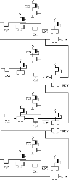
Its main job is to tell the instruction decoder which clock cycle of the current instruction is being executed. Instructions take at least 2 and at most 7 clock cycles, and the first cycle is always the fetch (loading the opcode into the instruction register).
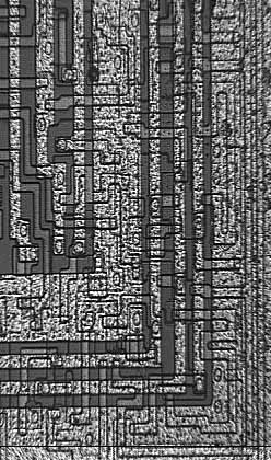
The timing generator reports 6 cycles, each on its own output, and these go straight to the PLA inputs. The last four cycles are implemented with a shift register in which a single circulating 1 bit carries the information; when RDY=0 the shift register acts as a 4-bit latch. The register also has a reset input, driven by the instruction decoder.
Interrupt logic
This block accepts interrupt requests arriving on the IRQ and NMI lines, decides whether they are enabled, and — once the processor reaches an instruction boundary — transfers control to the address held in the corresponding vector. On RESET it loads the reset vector.
All three cases are essentially an indirect jump, which needs memory read cycles. IRQ and NMI also need stack operations, because the flags and the program counter have to be saved. When an interrupt is accepted, the interrupt logic feeds a simulated BRK (software interrupt) instruction to the instruction decoder; the only difference between the events is the address of the jump vector.
While setting up the vector address it drives the address outputs directly. To do this it "reserves" clock cycles and stalls the rest of the processor with the internal READY signal (Rdy0 on the schematic). The other blocks see this as if a slow external device had pulled the RDY pin low, asking for extra clock cycles.
The three vectors — NMI, RESET and IRQ — are at FFFA, FFFC and FFFE. When a vector is loaded, the top 13 address bits are therefore 1 and the bottom 3 depend on the event. The lowest bit is always 0: it not only drives the address output, but also signals that interrupt handling is in progress. The circuit below uses this signal, and copies of it delayed by one and two clock cycles, to reserve the cycles needed to service the request:
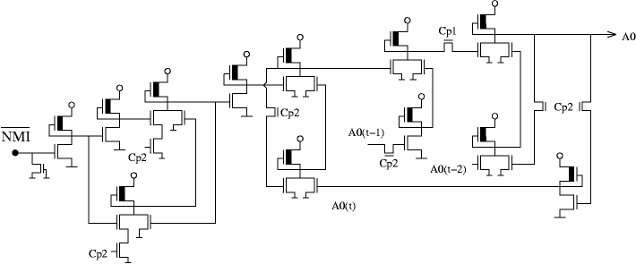
At first glance only the Schmitt-trigger NMI input seems to be wired directly to this circuit, but it works the same way for IRQ and RESET: the lowest address bit is 0 in all three cases, and its versions delayed by 1 and 2 clock cycles drive this circuit.
Register block: program counter
A 16-bit register inside an 8-bit processor, so it is built from two 8-bit halves and loading it takes 2 clock cycles. That is why addressing modes that work on the zero page (the lowest 256 bytes of memory) pay off: they save a clock cycle.
The most common operation on the program counter is incrementing it, so it has its own incrementer circuit. The ALU is not needed, and incrementing runs independently of the rest of the processor. The storage cells are inverter pairs fed back through the incrementer: if the carry is 0 the original bit is written back, if it is 1, its inverse.
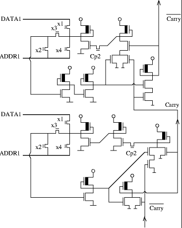
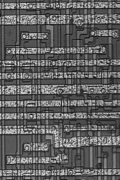
The transfer gates (the program counter is labelled IP on the schematics):
- x1 — write to the DATA1 bus, from where one 8-bit half of the PC can reach the data pins and the ALU
- x2 — load the PC from ADDR1 (when carry = 0)
- x3 — feedback
- x4 — write to ADDR1 (towards the ALU or the address outputs)
Stack pointer, X and Y index registers
In these registers a bit is stored in a cross-coupled inverter pair, with the loop broken by a transfer gate driven by a clock phase. During Cp1 the parasitic capacitances are charged; during Cp2 the loop closes and holds the information. The stack pointer can do one thing more than X and Y: its value can also be put on the address outputs.
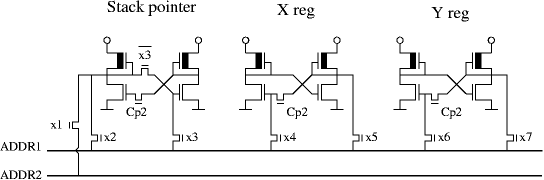
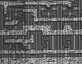
- x1 — write the stack pointer to ADDR2 (and from there to the address outputs)
- x2, x5, x7 — write to ADDR1 (to load other registers, or as an ALU input)
- x3, x4, x6 — read from ADDR1
Accumulator and BCD correction
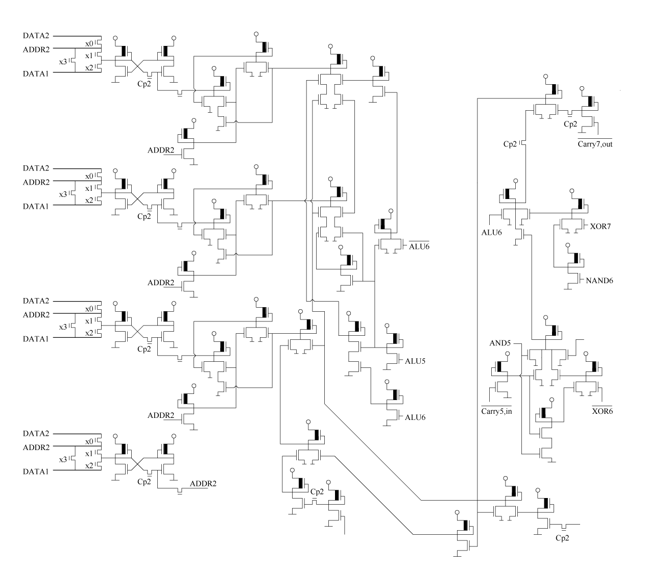
The accumulator receives its value through a BCD correction circuit. (Binary Coded Decimal is a number format in which, for example, the byte 33 — hexadecimal 21 — is treated as decimal 21: each 4-bit half of the byte holds one decimal digit.) Results of addition and subtraction must be corrected, because the ALU adds in binary. Both digits have to be checked for being greater than 9, and if so, 6 is added (that is how decimal 10 becomes hexadecimal 10).
The correction circuit below does this addition without a carry rippling through the bits — that would be slow and cost a clock cycle. Instead, it predicts the effect of the addition from the ALU's logic functions. The rightmost column of the circuit does the comparison, the second column from the right adds 6 when a digit is greater than 9 and BCD mode is enabled, and on the left are the 1-bit latches and adders.
Arithmetic and logic unit
The ALU is a very compact circuit. It sits inside the register block and uses the same internal buses as the registers. It has two input operands; the 5 transfer gates on the right of the schematic select which of the three buses, the complement of one of them, or 0 go to its inputs.
Regardless of the current instruction, the ALU always computes every logic function, the carry and the sum. Which of them reaches the output is decided by the transfer gates.
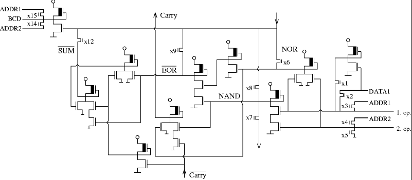
- Addition: reaches the output through x12. It needs a carry, which ripples through the 8 bits in alternating (true/inverted) logic.
- Subtraction: add the inverse of the subtrahend, with carry = 1 into the lowest bit.
- Comparison: a subtraction where x12 does not open.
- Increment: one input is 0, and the addition is done with carry = 1.
- AND, OR, EOR: switches x8, x6 and x9.
- Shift right: through x7 the output of the NAND gate goes to the inverted ALU output line of the next lower bit. This needs both inputs to be the same, i.e. the operand must be available on two buses.
- Shift left: multiplying by 2, which is an addition with two identical inputs.