Die layout
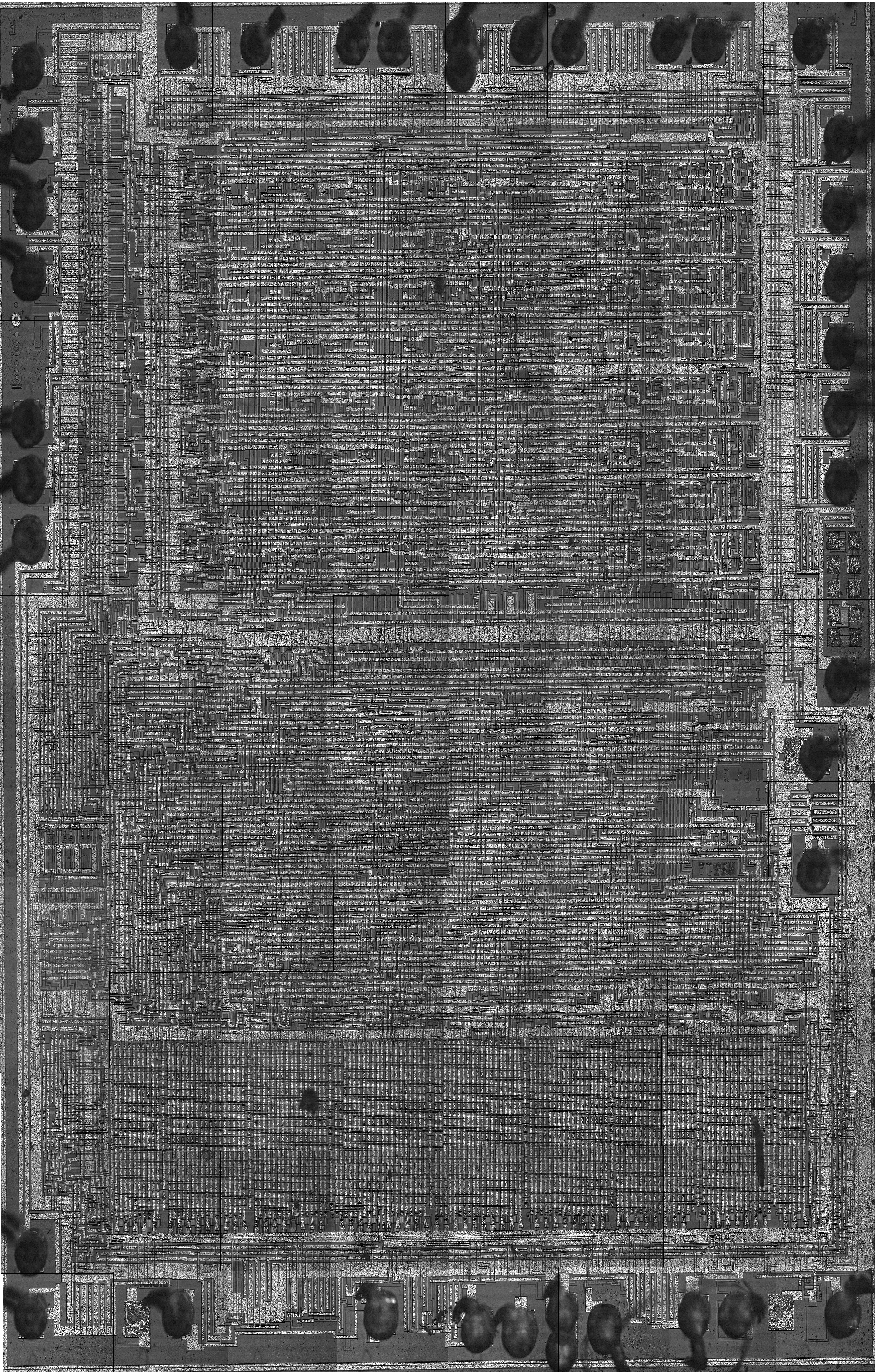
The complete 6502 die, stitched together from optical microscope images. Zoom all the way in to see individual transistors, contacts and the aluminium wiring.
How the image was made
The plastic package was removed by filing it down and dissolving the rest in hot, concentrated sulfuric acid. After rinsing, the bare die went under the microscope.
The first attempt used an electron microscope. It gave astonishingly detailed images — polysilicon wires and metallization showed up as crisp three-dimensional shapes — but the boundaries of the active (diffusion) regions were invisible, because there was no colour information. On an optical microscope those boundaries are clearly recognisable from the interference colours of the oxide (the nMOS primer explains why), so the work continued there.
The microscope's CCD camera produced 512×512 pixel frames. The whole die was digitised piece by piece and the frames were assembled in an image editor into the single 3634 × 5698 pixel picture above.
The layout is protected by copyright and must not be used directly for manufacturing. Looking at it, decoding it and taking ideas from it is fine — the images and schematics on this site can be downloaded freely.