Microprocessors: from layout to schematic
Download the original paper (Hungarian, Word, 2001)
Introduction
Since the 1960s the transistor has gone through breathtaking development, and the complexity of microprocessors still follows Moore's law today: the transistor count doubles every eighteen months. Competition between manufacturers is fierce. To win the trust of customers and investors it is not enough to put a good product on the market; getting technological innovations into the race as early as possible matters too, and it also makes marketing more effective. Who reached 1 GHz first? Which processor was the first to use copper instead of aluminium metallization?
Some manufacturers focus on running their products at the highest possible clock frequency; others work on reaching the highest computing performance cost-effectively. Besides manipulating customers, the market competition depends above all on development and trade secrets: very little is known about what actually happens inside a modern processor while it executes instructions. Manufacturers typically publish only the information that is strictly necessary to use the product.
This paper deals with the microscopic examination of processors and with the possibilities of decoding their schematic from layout photographs. I analyse one concrete case in detail: the complete reverse engineering of the 6502. This processor represents a very important stage of the development: the first Hungarian personal computers were built on the 65xx family, which is a model of cheap, efficient and inventive design. Its size and simplicity make it possible to publish its circuit diagram drawn on a single large sheet, so it can serve as an illustrative teaching aid for people working in microelectronics. I also cover a phenomenon that is common in other processors as well: undocumented instructions — how they work, what they can be used for, and why they exist at all.
Based on this experience I examine whether Intel x86 processors could in principle be decoded, and summarise the applicable methods. Beyond teaching, the results have practical relevance. On the one hand, failure analysis of integrated circuits requires transistor-level examination; on the other hand, during design, reverse engineering the layout before manufacturing can verify whether the circuit implements the intended function. This procedure is part of the verification steps used in design.
An overview of the 6502
The success story of the 6502 began with the Apple II; in Hungary it is known mainly through the Commodore machines. Its operation and programming are almost identical to the 6510 found in the very first Commodore 64s; the difference is that a few bugs were fixed in the 6510 and it was given 6 I/O pins. The 6502 was used in the VC1541 disk drive. Today it may seem odd that a floppy drive needs an 8-bit processor with the same computing power as the computer itself. The VC1541 is a separate unit, an intelligent peripheral connected over a serial bus, with 2 KB of freely programmable RAM (used by special disk routines and fast loaders that drove the reading and the stepper motor directly).
The members of the 65xx family have a minimal number of registers, but thanks to the many addressing modes these can be used very efficiently: a 16-bit program counter (IP), an 8-bit stack pointer (SP), the flags, the accumulator (A), and the X and Y index registers. Stack operations and instructions working on the lowest 256 bytes of memory are one clock cycle faster than other operations, and speed-optimised software takes advantage of this. Simple instructions complete in 2–3 clock cycles. The indirect indexed and indexed indirect addressing modes are notable: they allow very efficient data-manipulation loops. BCD arithmetic is also supported, and with a better solution than in today's PC processors: no separate instruction (DAA) is needed to request the correction, because it is automatic once the D bit is set in the flags, and it costs no extra clock cycle. Instructions are 1, 2 or 3 bytes long, and they produce very compact code: the BASIC interpreter in the Commodore 64 ROM, for example, is only 8 KB.
56 instructions, 13 addressing modes. Despite its efficiency, the 65xx family was much cheaper than its competitors, and it held its own even against the first 16-bit processors.
The layout
The plastic package was removed by filing and with hot, concentrated sulfuric acid. After rinsing, the silicon die went under the microscope. I tried an electron microscope first. It gave astonishingly detailed images; the polysilicon wires and the metallization appeared as clearly visible three-dimensional shapes. The boundaries of the active regions, however, were not visible at all, because there was no colour information. Why integrated circuits are colourful even though silicon is grey: during manufacturing the parts of the circuit — transistor gates, polysilicon wires, active regions, metallization — are formed in a fixed order. An insulating layer is needed to separate the parts; this is silicon dioxide. The oxide grows in a high-temperature furnace, and since each part spends a different amount of time in the furnace, the oxide grows to a different thickness depending on what is underneath. Light reflected from the surface of the oxide and from the oxide–silicon interface interferes, and the colour depends on the oxide thickness and on the viewing angle. In any case, the boundaries of the components are visible, which helps enormously in decoding the circuit.
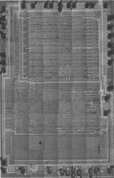
So I continued on an optical microscope fitted with a CCD camera. The resolution was far from as good; being a mid-range microscope, it produced images from which decoding was only just possible. The active regions, however, were easy to recognise by their colour, so I could start the work. The CCD camera produced 512×512 bitmaps; I digitised the whole die in small pieces and assembled them with an image editor.
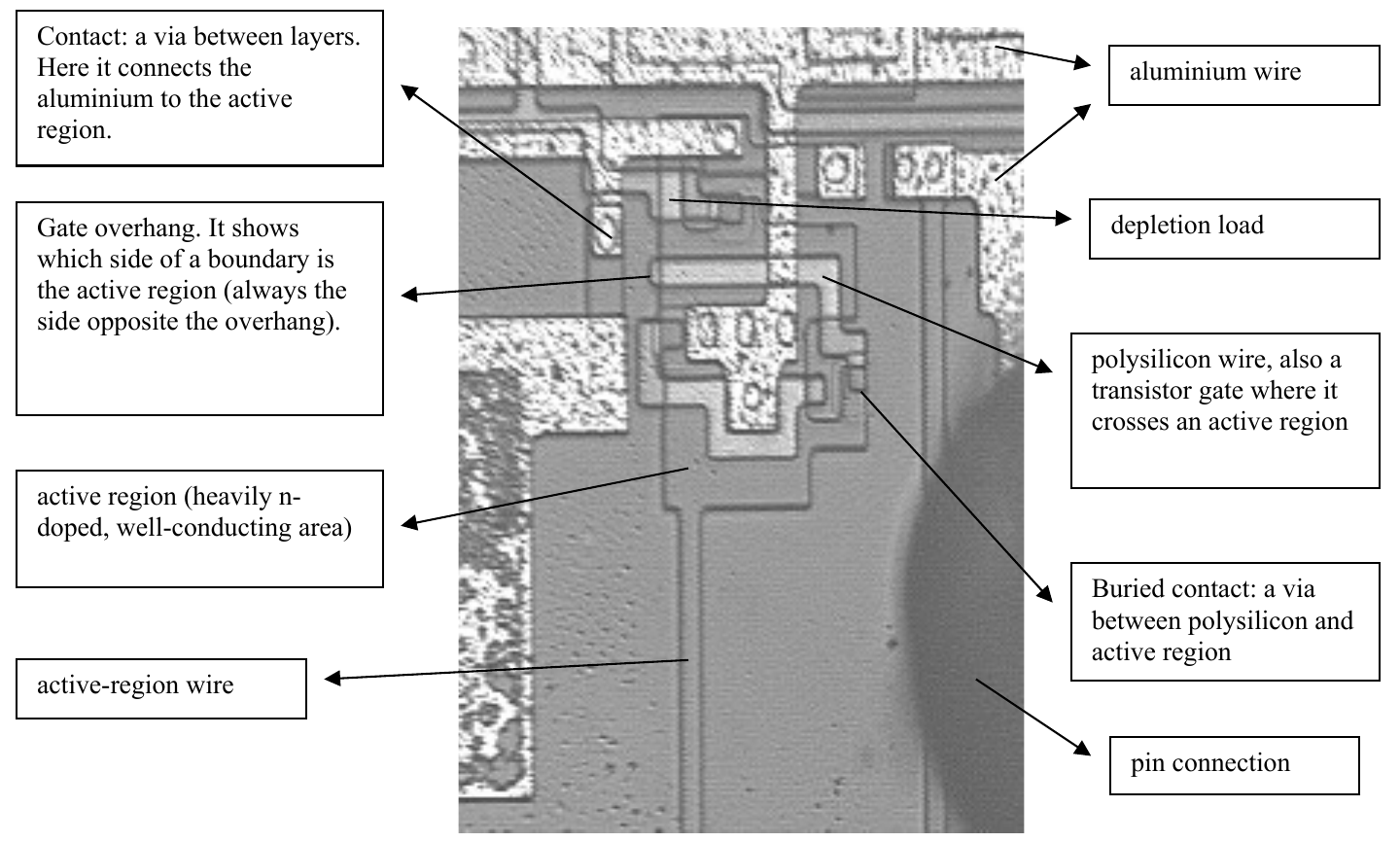
The basic shapes from which the circuit can be reconstructed are the following:
Transistors
- Depletion mode: the load transistor of every gate is of this type. It can be recognised by its characteristic shape, and by its drain being on the supply and its gate tied to its source.
- Enhancement mode: everything other than the load transistors.
Wires
- Aluminium: light grey. It can cross the other two wire types, since there is oxide between them. Supply and ground reach everything through aluminium wires.
- Active region: dark grey. Inside the 6502 it is very rarely used as a wire.
- Polysilicon: the most common wire type, since it also forms the transistor gates. The output of a gate and the input of the gate it drives can be a single polysilicon wire; the role of the polysilicon depends on the boundaries of the active regions.
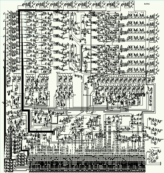
The complete layout (Figure 1) splits into three clearly separate parts: the register block, which visibly consists of 8 rows; a very tangled mass of transistors in the middle; and finally a PLA, which is the most regular structure. The component set consists solely of transistors and wiring — there are no capacitors either, even though the processor contains a large number of dynamic storage nodes. The capacitance they need comes from the transistors and the wires.
Supply and ground reach the gates everywhere through aluminium wires. So do the clock lines that span long distances, with one exception worth mentioning: in the middle section of a long aluminium wire, one of the clock phases travels on double-width polysilicon. The designers were forced to interrupt the aluminium, and they tried to compensate for the higher resistivity with the double width.
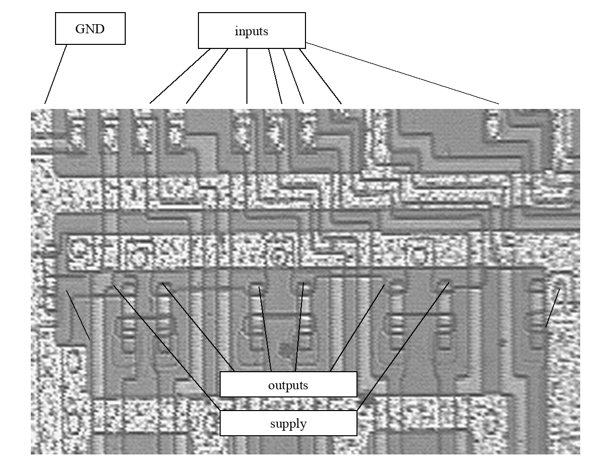
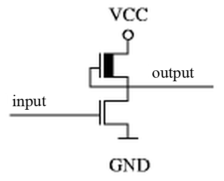
There is hardly any regularity in the shape of the gates; a wide variety of forms can be seen. The loads and the inputs of some gates are very far apart on the layout — a downside of the patched-together design. One gate even has its load connected to its driver transistors through a long polysilicon wire, which probably hurts its switching characteristics. In all this variety only one rule can be recognised, concerning the number of inputs: a NAND gate has at most 2 inputs, a NOR gate at most 8.
At the edge of the layout there are also test circuits, with large metal areas for attaching probe needles.
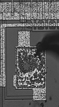
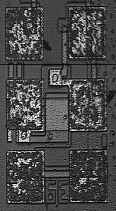
Another trace of the development process: an aluminium wire was patched with a piece of polysilicon at a place where nothing crosses it, which seems pointless. Surely in an earlier design phase another aluminium wire crossed it there and was later moved elsewhere. Bit 5 of the flags is similar: its write line is "hanging in the air". This bit is unused and always reads back as 1. Wires interrupted by transfer gates also pass through inverters (signal regeneration); the only notable exception is the driver circuit of the upper 8 address outputs, where 3 transfer gates are connected in series.
Fortunately there is no metallization covering large areas anywhere on the layout, so every transistor is clearly visible. (Otherwise the metallization would have had to be etched away, as Figure 6 shows: a photo of an Intel 8255 peripheral controller.) The 6502 uses its area exceptionally well; there is no free space anywhere — the economical design is striking.
Decoding the schematic
I started with the register block, because it looked the simplest, and since it consists of repeated rows, I could map a large area of the processor relatively quickly. The 8 bit rows are not entirely identical — for example the carry is passed along in alternating logic, so some circuits are implemented as their dual in every other row. The columns, as separate registers, resemble each other only slightly: what they have in common is that each stores its information in a cross-coupled inverter pair broken by a clock-controlled transfer gate; the difference is that, depending on their function, the registers can write to or read from different internal buses. The Arithmetic and Logic Unit is also a separate column in the register block.
Once the block was decoded, I knew how the registers and the ALU exchange data and how this is written to the D0..D7 pins of the processor. Then I noticed that these 8 data bits also reach the inputs of the PLA, so it seemed obvious that the PLA plays a role in instruction decoding. I numbered the columns and rows and created a table of ones and zeros. A program processed this table and, knowing the complete instruction set, calculated for every NOR gate which instructions make its output 1 (this is not unique: if neither the true nor the complemented line of a data bit is connected to the gate, several opcodes can activate the output). For easy handling the program produced its results as an HTML file: with it you can quickly find out which instructions a PLA output affects, and which PLA outputs are active while a given instruction runs. Links let you move between the two lists, so this format speeds up processing the results and makes the data set easier to survey.
Then came the hardest part of the work: the most tangled, central area of the layout, which is also the heart of the operation — 138 inputs from the PLA, 40 outputs towards the register block. I printed the whole thing on A4 sheets, drew the decoded circuit fragments, numbered the wires and wrote the numbers on the edges of the A4 layout images. It was somewhat confusing that the processor was designed in a patched-together way, so circuits belonging to the same function (e.g. the interrupt logic) do not form one contiguous area on the layout but are scattered around. What's more, there are even gates whose inputs are on one sheet while their load is two sheets away, connected by a long polysilicon wire. Because of this it took a month and a half to find every transistor on the layout. The result did not resemble a schematic at all — just a tangled heap of gates with a multitude of wire definitions like F4X12, G3X15 and so on.
There is an area almost completely covered by metal, and the image of it was so poor that it took me 2 days to decode those 20–30 transistors. From the image it was not clear what connects to what; several possibilities came up, so the function had to be taken into account as well. I excluded every case in which a gate would have been left without a load, or a gate would have had an undriven input. Only one case remained, and fortunately it fit perfectly into the circuit functionally too, so I have no reason to think I decoded it wrongly.
I made the first drawing of the circuit: I put the many small pieces together and connected whatever I could. The result was a completely unreadable drawing; only the status register had all of its circuitry in one heap. Whatever I could not connect on the sheet I marked with the usual wire number. That is when I realised my naming scheme was flawed: I had given the same name to wires carrying the same information, but I had not changed the name at every transfer gate, which may also mean a time shift. So some identically named things on the drawing cannot actually be connected. I made the second drawing like this: I tried to gather the circuits belonging to the same functional group, so I jumped all over the layout and checked every wire for transfer gates. The first drawing served only to check whether my function-driven wandering had reached every transistor.
The third, final drawing was no longer made on paper but on a computer, using a Unix drawing program called Xfig. Aesthetics drove its design: the blocks had to be placed so the sheet was well filled and as many wires as possible were drawn in, without the drawing becoming tangled — above all, the finished schematic had to be easy to follow, so that you can see which parts of the processor an instruction sets in motion and in what order.
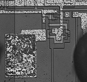
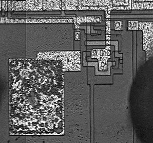
An interesting feature of the test pad in the figure is that it is not connected anywhere, yet its aluminium surface is damaged, as if it had been probed with a needle. The metallization is not damaged anywhere else on the layout, only at test pads like this one. Probably measurements of the oxide properties were made on it.
How the processor works
The block diagram published by the manufacturer is a simplified picture of reality: far more lines run between the blocks than the 1-bit and 8-bit wires it shows, and there are connections between blocks that are not drawn at all.
First, let's see roughly how an instruction is executed. The fetched opcode goes into the instruction register, an 8-bit latch, and the value stored in it is used in every clock cycle throughout the execution. A shift register counts which clock cycle the execution is in. The outputs of this and of the instruction register feed the inputs of a PLA, which takes part in instruction decoding. The PLA has 138 outputs. Some have a simple meaning (e.g. TSX instruction in the second clock cycle: this line goes through a push-pull inverter straight into the register block and controls 8 transfer gates that write the contents of an internal bus into the X register), but some outputs are quite complex, standing for groups of instructions, and several of these are processed by a combinational network. Of course, the instruction decoder gets inputs not only from the PLA and its combinational network, but also from the interrupt logic and the status register (for conditional branches), and it uses quite a few internal control signals that are not on the block diagram at all, such as the internal Ready signal or the Sync signal.
The operations are actually carried out in the register block. There are 4 internal buses through which the registers and the ALU exchange data. Transfer gates, controlled by the instruction decoder, steer the data flow and select which of the arithmetic results the ALU produces in a phase reaches its output. Writing any register takes 1 clock cycle (precharge in phase Cp1, evaluation in Cp2). Incrementing the program counter runs in parallel with all other operations, because it has its own adder. Indexing goes through the ALU, and so does BCD correction, which does not even need an extra clock cycle.
Clock generator
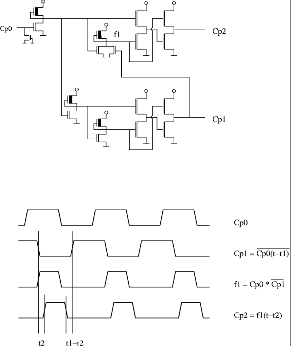
From the Cp0 clock input (980 kHz) the processor itself generates the Cp1 and Cp2 phase signals. They never overlap, so they divide every clock cycle sharply into two time slices. This is useful not only for writing the registers — external devices may need it as well, so both phases are brought out to pins. The essence of the clock generator is that two push-pull inverter pairs, which deliver large currents (the phase signals have to reach everywhere) and are slow, are used as delay elements to shift the signals in time, as shown in the figure below. The circuit itself is very simple and uses few transistors, but it occupies a lot of silicon area, like the bus drivers.
Instruction decoder
Its core is the PLA, built from NOR gates, which takes its inputs from the instruction register and the timing generator. Its outputs drive the register block directly. Another important task is determining instruction boundaries: this is needed to issue the fetch signal, to drive the SYNC pin, and for the interrupt logic (interrupts are taken only at instruction boundaries). When a new opcode has to be fetched depends on the previous opcode, because most instructions take a fixed number of clock cycles, whether or not there is BCD correction. The exceptions are conditional branches, where, depending on whether the condition holds, either a jump or a fetch follows.
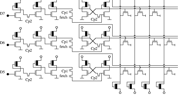
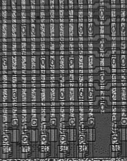
On the layout the columns are the outputs of the NOR gates and the rows are the true and complemented inputs. The arrangement is quite practical, because one contact can carry two bits of information: the complemented input of one row and the true input of the row below it. The 8 data-bit inputs, incidentally, are not in order but scrambled. Some columns are not contacted anywhere, for example because they do not belong to the instruction decoder at all but carry the IRQ request.
The PLA outputs are received by a combinational network which works not only from the PLA but also uses quite a few internal control signals, such as the internal Ready signal, the Sync signal, and one of the timing generator outputs. Passing through complex gates, the PLA outputs reach push-pull inverters which drive a long polysilicon line and 8 transfer gates, directly controlling the reading and writing of the registers, the operation of the ALU, and the contents of the bus drivers and the address and data lines.
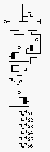
Figure 11 shows a simple case: the control for writing the accumulator. PLA outputs 61 to 66 gate the following operations: writing X or Y to A, logical operations, addition/subtraction, shifting the accumulator, and loading it from the stack. There are, however, much more complicated circuits that also control the transfer gates of the register block, for example deciding when to copy one internal bus onto another, where the ALU takes its inputs from, and so on. Gates with many inputs process those PLA outputs that are not fully specified: some bits of the opcode are tied neither to 0 nor to 1. Because of this, unused opcodes can produce quite interesting behaviour. Since nothing checks whether an opcode is valid, something always happens: some PLA outputs become active, and the register block does something in response. The so-called "illegal opcodes" fall into three groups:
- No-op, like NOP: it reads its operand and writes it to a bus, but then finishes and "forgets" the result. A later instruction will overwrite it, so it is lost.
- Meaningful instruction, which can be complex and perform several operations, for example ANE:
A = (A | #$EE) & X & #byte. Even the built-in constant is not guaranteed! - Instruction that freezes the CPU. If the contents of several registers are written to the same bus, or several of the logic functions the ALU computes in one pass are forced onto its output, logic gates may fight each other and no clean 0 or 1 level develops. The following gates accept it and make something of it, but they always switch more slowly. The required timing falls apart and the processor ends up in an inoperable state.
Illegal opcodes had an important application in copy protection, as one of many methods software authors used to make crackers' work harder. Early disassemblers did not know the illegal opcodes and displayed them as invalid, so they also determined the instruction boundaries incorrectly: a program written with illegal opcodes looked like a confusing heap of bytes that was hard to modify.
Timing generator
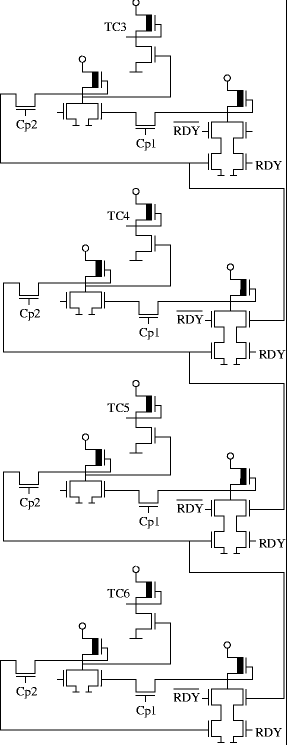
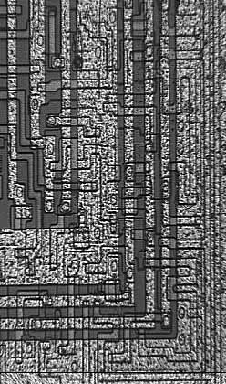
Its main task is to tell the instruction decoder which clock cycle of the current instruction is being executed. Instructions take at least 2 and at most 7 clock cycles, and the first cycle is always the fetch (loading the opcode into the instruction register). The timing generator outputs the information for 6 cycles, each on its own output (these go directly to the PLA inputs). The last four cycles are implemented with a shift register in which a single circulating 1 bit carries the information; when RDY=0 the shift register works as a 4-bit latch. The register also has a reset input, driven by the instruction decoder.
Interrupt logic
Its task is to accept interrupt requests arriving on the IRQ and NMI lines, decide whether they are enabled, and — once the processor reaches an instruction boundary — transfer control to the address given by the corresponding vector, and on RESET to load the reset vector. All three cases are essentially an indirect jump, which needs memory read cycles. IRQ and NMI also need stack operations: the flags and the program counter have to be saved. When an interrupt is accepted, the interrupt logic simulates a BRK (software interrupt) instruction to the instruction decoder; the only difference between the events is the address of the jump vector. While setting the vector address it drives the address outputs directly; for this it "reserves" clock cycles and stalls the rest of the processor with the internal READY signal (Rdy0 on the schematic). The other blocks perceive this as if a slow external device had pulled the processor's RDY pin low, asking for extra clock cycles. The three vectors — NMI, RESET and IRQ — are FFFA, FFFC and FFFE respectively. So when a vector is loaded, the top 13 address bits are 1 and the bottom 3 depend on the event. The lowest bit is always 0; it serves not only to drive the address output but also to signal that interrupt handling is in progress. The circuit below uses this signal, and versions of it delayed by clock cycles, to reserve the clock cycles needed to service the request:
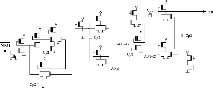
Although at first glance only the Schmitt-trigger NMI input appears to be connected directly to the circuit above, it works the same way for IRQ and RESET, since the lowest address bit is 0 in all three cases, and this signal delayed by 1 and 2 clock cycles drives the circuit.
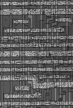
Register block: program counter
A 16-bit register inside an 8-bit processor: it was implemented in two 8-bit halves, and loading it takes 2 clock cycles. Addressing modes working on the so-called zero page (the lowest 256 bytes of memory) are advantageous, because they save 1 clock cycle. The most frequent operation on the program counter is incrementing it; a separate circuit is built in for this, so the ALU is not needed and incrementing runs independently of the rest of the processor. The storage cells are inverter pairs fed back through the incrementer: if the carry is 0 the original bit is written back, if it is 1, its inverse.
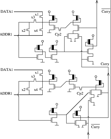
The transfer gates (the program counter is labelled IP):
- x1: write to the DATA1 bus, from where one 8-bit half of the IP can reach the data pins and the ALU
- x2: load the IP from ADDR1 (when carry = 0)
- x3: feedback
- x4: write to ADDR1 (towards the ALU or the address outputs)
Stack pointer, X and Y index registers
In these registers a bit is stored in a cross-coupled inverter pair broken by a transfer gate driven by a clock phase. During Cp1 the parasitic capacitances are charged; during Cp2 the loop is closed and holds the information. The stack pointer can do one thing more than X and Y: its value can also be written to the address outputs.
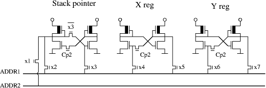
- x1: write the stack pointer to ADDR2 (and from there to the address outputs)
- x2, x5, x7: write to ADDR1 (to load other registers, or as an ALU input)
- x3, x4, x6: read from ADDR1
Accumulator and BCD correction
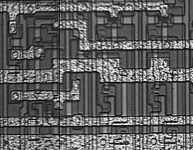
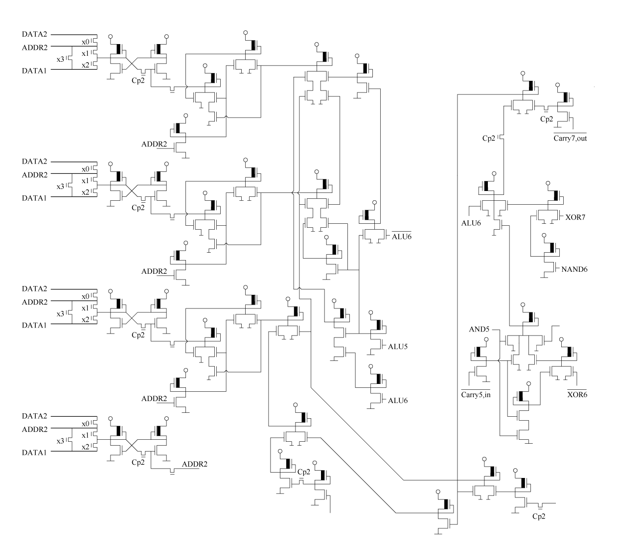
The accumulator receives its value through a BCD correction circuit. (Binary Coded Decimal is a number representation in which, for example, the byte 33 — hexadecimal 21 — is processed as decimal 21, i.e. each 4-bit half of the byte holds one decimal digit.) The results of addition and subtraction must be corrected, because the ALU performs binary addition. Both digits must then be checked for being greater than 9, and if so, 6 must be added (that is how decimal 10 becomes hexadecimal 10). The correction circuit below performs this addition without a carry rippling through the bits — that would be slow and cost a clock cycle — and instead predicts the effect of the addition from the ALU's logic functions. The rightmost column of the circuit does the comparison, the second column from the right adds 6 when a digit is greater than 9 and BCD is enabled, and on the left are the 1-bit latches and adders.
Arithmetic and logic unit
The arithmetic and logic unit is a very compact circuit. It sits in the register block and uses the same internal buses as the registers. It has two input operands; on the right side of the schematic are the 5 transfer gates that select which of the three buses, the complement of one of them, or 0 go to the inputs. Regardless of the current instruction, the ALU produces every logic function, the carry and the sum. Which of them reaches the output is decided by the transfer gates.
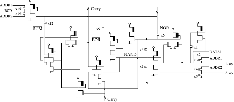
- Addition: reaches the output through x12; it needs a carry, which propagates through the 8 bits in alternating logic.
- Subtraction: adding the inverse of the subtrahend, with carry = 1 into the lowest bit.
- Comparison: a subtraction, except that x12 does not open.
- Increment: one input is 0, addition with carry = 1.
- AND, OR, EOR: switches x8, x6, x9.
- Shift right: through x7 the output of the NAND gate goes to the inverted ALU output line of the next lower bit. This requires both inputs to be the same (i.e. the operand must be available on two buses).
- Shift left: multiplication by 2, which is an addition of two identical inputs.
The finished schematic
I tried to make the drawing as easy to follow as possible, and this forced a few compromises:
- Except for the register block, the schematic has little to do with the arrangement of the layout.
- Not every wire is drawn. In the rows of the register block, the internal buses DATA1, DATA2, ADDR1 and ADDR2 run through every register. The complemented Rdy0 signal is used in very many places, so it is only marked (its value is set by the interrupt logic and by the circuit generating the Sync and R/W signals). In the middle of the schematic, the outputs of the push-pull inverters cross all 8 rows of the register block; they are named x5, x12 and so on. Their numbering restarts under every register!
- The rows of the PLA are shuffled on the layout; on the schematic they are sorted.
The Intel 80286
The next subject of my investigation was this part, made in a 1.2 micron process. It contains about 110,000 transistors and, like the 6502, uses nMOS technology with depletion loads. Its layout is fundamentally different from the 6502's: it is well structured and was designed by computer. Circuits belonging to the same function sit together in one block, the 16-bit repetition shows up as 16 identical layout groups, there is even some empty space, and the structure is completely clear.
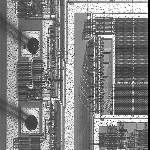
In the 6502, by contrast, the 8 bits of the instruction register do not all look the same (and of course they are not laid out in order but scattered about); the circuits of two bits are crammed into a corner of the layout simply because that is where there was room. This is not a viable approach for more modern processors. Firstly, it is inefficient: the differing circuits each have to be simulated again, instead of placing one cell side by side 8 or 16 times. Secondly, layout differences can cause differences in speed and timing, which is unacceptable at high clock frequencies.
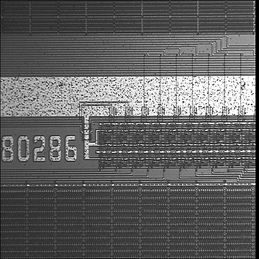
The other striking feature of the 286 layout is the large number of PLAs. These can be used as ROMs, for example for instruction decoding, and blocks of NAND and NOR gates can also be turned into state machines by feeding outputs back to inputs: from the inputs and the previous states, delayed by the clock, the PLA generates the logic functions that set the outputs and the next states. This is a compact, area-saving solution, because it is a regular structure — a matrix in which each 1-bit cell depends only on whether there is a contact or not. It is also simple to design, but the large internal capacitances make the finished circuit slow. In later members of the 80x86 family the PLAs were replaced by combinational logic. That takes up far more silicon area, but it is the price of high-speed operation.
Could the 286 be reverse engineered completely? The experience gained with the 6502 allows an estimate of the effort. Roughly 30 times as many transistors does not mean anything like 30 times the work: thanks to the systematic design, once the transistors have been recognised there is no need to untangle and rearrange the circuit, and being a 16-bit processor it has far more repeated circuitry. On top of that, PLAs make up a quarter of the layout, and an even larger share measured in transistors. Under these conditions an experienced team of 4–5 people could decode it in a few months. Whether it is worth doing is another question. The Amiga is a good example: a few years ago, after Commodore's bankruptcy, there was an attempt to bring it back to life. The planned new model had to be compatible with its predecessors, but the design drawings of one of the ICs had been completely lost. It was reverse engineered...
Decoding processors of this level is therefore possible, although of course the size and complexity make it impossible to produce a single, coherent schematic.
Later members of the x86 family
From the 386 onwards only CMOS technology was used, so the circuits contain both n-channel and p-channel transistors. This makes decoding the layout considerably harder, because the two cannot be told apart unambiguously from the image. Fortunately there are a few clues:
- CMOS circuits mostly contain complementary p networks: the gates are built so that the p transistors can be inferred from the n-channel ones, because their connection is the dual of the n network.
- The p inversion layer has lower conductivity, so p-channel transistors are 2–3 times wider than an n-channel transistor delivering the same current.
- Once a transistor is somehow found to be n or p, every transistor in the same well is known as well.
![CMOS layout photo [8]](/static/chip6502/paper/fig23_en.png)
![CMOS layout photo [8]](/static/chip6502/paper/fig24_en.png)
These rules are useful, but they do not guarantee an unambiguous result. For CMOS it is much more true that you can only decode it if you also understand how the circuit works. In some cases the type of a transistor can only be determined by examining the operation. With nMOS such methods are needed only when the layout photo is poor or contamination hides components.
With its 1-micron feature size, the 386 can still just about be examined with a conventional optical microscope. Smaller features are comparable to the wavelength of light. Newer dies with even smaller feature sizes can be examined with a scanning electron microscope or a scanning optical microscope. The SEM gives no colour information, i.e. the boundaries of the active regions cannot be recognised in the image, so it cannot be used on its own. Selective etching has to be applied, which is needed for newer circuits anyway, for example because of multi-layer metallization. Taking images of a transistor layer in several planes causes very serious registration problems. It is unavoidable that the wafer is moved between the various etching and microscopy steps, and the unevenness of the wafer and the imperfect levelness of the slide always cause misalignment. This can be critical, since even a 1-micron offset can cause errors spanning several transistors. Near-field scanning optical microscopy is quite expensive and currently not available in Hungary. Its principle is that the surface is scanned with an optical fibre whose aperture diameter and distance from the surface are both smaller than the wavelength of light.
So with conventional methods you can get as far as the 386, i.e. technology from about 15 years ago can be dissected without great expense. But even these circuits are complex enough to give anyone attempting to decode them plenty of work: the 386, for example, has 275,000 transistors. With a component count of this magnitude, only software-based layout decoding is conceivable. The idea is that software processes the layout photos, recognises areas of the same shade (function, material), and maps them, for example, into a graph based on the adjacency of the areas and the positions of the contacts. It could even generate a schematic from this, although fully automatic operation would be a very hard artificial intelligence problem. The practical way is surely software-assisted decoding: a human operator organises the machine-generated data into a schematic, taking into account how the circuit works.
References
- Dr. Imre Mojzes: Mikroelektronika és elektronikai technológia (Microelectronics and electronics technology). Műszaki Könyvkiadó, 1995
- Dr. Ferenc Kovács: MOS integrált áramkörök (MOS integrated circuits). Műszaki Könyvkiadó, 1976
- János Saufert: Mikroprogramozás és mikroprocesszorok (Microprogramming and microprocessors). KGTMT, 1977
- Zoltán Simon: Második generációs mikroprocesszorok felépítése… (The structure of second-generation microprocessors and benchmark programs for the Intel 8080, Motorola 6800, Signetics 2650 and Fairchild F-8). HIKI, 1977
- Angerhausen–Brückmann–English–Gerits: A Commodore 64-es belső felépítése (The anatomy of the Commodore 64). Data Becker – Novotrade, 1985
- http://www.6502.org
- http://www.intel.com/intel/intelis/museum/exhibit/hist_micro/hof/hof_main.htm
- http://www.eet.bme.hu