Reading an nMOS layout
A guide for anyone with minimal electronics background: how an integrated circuit works, and — with detailed explanations — how to decode a layout yourself. All images come from the 6502.
Technology basics
Integrated circuits are built on a slice of single-crystal silicon. In high-temperature furnaces the silicon is doped with various impurities, which change its conductivity and other properties. Patterns are created with photolithography: a light-sensitive resist is applied to the surface and exposed through a mask; how easily the resist dissolves afterwards depends on whether it was hit by UV light, and then the exposed areas are etched.
Wiring is done in polycrystalline silicon and a metal layer (usually aluminium; more recently copper as well). Components are separated by an insulating layer of silicon dioxide.
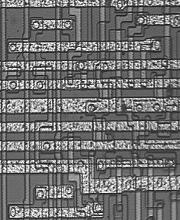
If you look at a chip — with the naked eye or under a microscope — it shimmers in all sorts of colours, and the colours change with the viewing angle, even though silicon itself is a uniform grey. The explanation: during manufacturing the parts are formed in a fixed order (thin oxide, polysilicon wires and transistor gates, active regions, metallization). Because each part spends a different amount of time in the furnace, the oxide grows to a different thickness depending on what is underneath. Light reflected from the top of the oxide and from the oxide–silicon interface interferes, and the colour depends on the oxide thickness and the viewing angle. Either way, the boundaries of the components are clearly visible, and that helps enormously in decoding the circuit.
The nMOS transistor
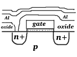
Here is what an nMOS transistor looks like in cross-section:
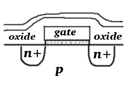
The image shows n+ doped regions formed in a p-type substrate, with a thin oxide on the silicon between them (the dotted area) and polycrystalline silicon on top of that. Everything is covered by oxide and a passivation layer. The two n+ regions are the transistor's source and drain (their order does not matter here — the structure is symmetrical), and the polysilicon is the gate.
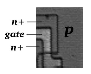
This is the same transistor under the microscope. You can clearly see the dark line marking the edge of the active (n+) region between the p and n+ areas, and the Z-shaped polysilicon wire, which is also the transistor's gate.
The first and most important rule of layout decoding: there is a transistor wherever a polysilicon wire crosses an active region. The p and n+ areas have the same colour, only their boundary is distinct — but with a rule described further below, this will not cause problems either.
Now add the aluminium wire to the cross-section. Above one of the electrodes the oxide is opened, so there is a connection between the transistor electrode and the aluminium wire. The aluminium and the polysilicon wires cross each other, but there is no connection between them — the oxide prevents it.
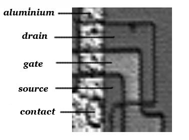
The light grey vertical line is the aluminium. It crosses the transistor and connects to the source electrode through a contact. The round area is the contact; underneath is an active region (which you can only infer from the region boundary, not from the colour). Areas hidden under large metal surfaces can sometimes be difficult to decode.
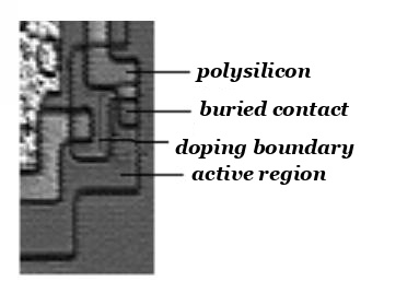
Another type of contact is the buried contact, which connects an active region directly to polysilicon. To keep such a junction from behaving like a rectifier, an extra doping step is used — you can see it on the layout image.
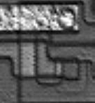
Finally, the last shape you need for nMOS layout decoding: the depletion-mode transistor. Every logic gate has one. Its gate is always tied to its source, and its drain is always on the supply. On this layout the aluminium wire is +5 V, and the gate is connected back to the source through a buried contact.
Recognising these shapes is enough to decode an nMOS integrated circuit built from depletion-load gates.
Basic digital circuits
MOS transistors are used in analog circuits too, but their real home is digital logic. To get a working understanding of the MOS transistor and the circuits built from it, you need neither atomic physics nor voltage–current characteristics. As a first approximation, a MOS transistor is a switch: the voltage on the gate decides whether current can flow between the other two electrodes.
Apart from wiring, the 6502 contains nothing but enhancement-mode and depletion-mode transistors. Their circuit symbols:
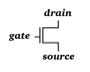
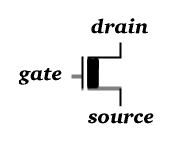
The most important basic circuit is the inverter, which is also the most common gate in these processors. It is used for much more than inverting:
- delay
- signal regeneration (an even number of inverters on a long wire)
- storage (cross-coupled inverters)
- amplification (push-pull inverters at the chip's pins)
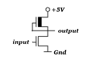
The inverter is a two-transistor circuit. The lower (driver) transistor either pulls the output down to 0 or not, depending on the input. If the input is logic 1 (e.g. 5 V), the driver turns on and shorts the output to ground, so the output is logic 0. If the input is 0, the driver is off (as if it were not there), and the output is pulled up to 1 through the load transistor — which is always on, since its gate is tied to its source. Of course the load is also on when the input is 1 and the driver conducts. The designers size the channel widths so that the two transistors do not simply fight each other, and the output switches decisively when the input goes from 0 to 1 (the driver is the stronger one).
Every other logic gate works on the same principle. Each gate's output comes from a depletion load (so every gate has an inverted output), and the arrangement of the input transistors — series or parallel — determines the logic function. If two inputs drive transistors in parallel, the output is pulled to 0 when one OR the other input is 1; with the inverted output, that is a NOR gate. If the input transistors are in series, both one AND the other must conduct to pull the output down: that is a NAND gate.
There are also complex gates with many inputs in series-parallel arrangements; their function follows easily from the NAND and NOR logic.
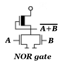
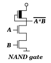
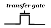
A transfer gate switches the flow of data on a line: it is a transistor inserted into the data path with its source and drain. When its gate gets logic 1 (e.g. 5 V) it acts as a short and lets data through. With logic 0 it is an open circuit, so the state on its output side does not change. (It is symmetrical, too: which side is the output is decided by which side is connected to a gate input.)
No more than three transfer gates are ever placed in series, because each one degrades the signal level (by the MOS threshold voltage). If more are needed, an even number of inverters is inserted into the path to regenerate the signal.
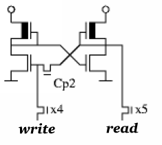
The 1-bit latch in the figure is taken from the 6502. A cross-coupled inverter pair does the storing: the information enters the input of one inverter, and after two inversions the unchanged bit returns to the same input through the feedback path.
The feedback path contains a transfer gate driven by Cp2 so that the feedback only acts in the second half of the clock cycle and not all the time — otherwise flipping the latch would be difficult, with the inverters fighting each other.
The latch is written and read by switching the x4 and x5 transfer gates on the respective lines.
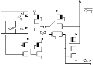
A storage element does not have to be built from inverters: any complex gate whose output is fed back to its input with the right timing will do. The flags in the 6502 work exactly this way.