Reverse engineering the 6502, revisited
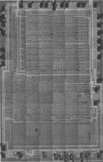
Back in 2001, as an electrical engineering student at the Budapest University of Technology, I spent several months taking apart a MOS 6502 — not the software kind of taking apart, but literally: dissolving the plastic package in hot sulfuric acid, photographing the bare silicon under a microscope, and tracing every one of its roughly 3,900 transistors back into a schematic.
The result became a student research paper (Microprocessors: from layout to schematic) and a small website written in PHP3, in Hungarian. That site has been gone for well over a decade, yet every now and then someone still reaches out to ask me about it. Proof, if any was needed, that the internet never forgets.
So I've rebuilt it, in English:
 Inside the 6502 →Zoomable die photo, the full schematic, and how each block works.
What's there
- Die layout — the complete die, stitched together from 512×512 pixel CCD frames, now in a deep-zoom viewer instead of the old click-through grid of thumbnails.
- Schematic — the full transistor-level schematic. The old site apologised that there was no zoomable web version; now there is, rendered straight from the original xfig drawing.
- Circuits — the clock generator, the PLA-based instruction decoder, the timing generator, interrupt handling, the register block, BCD correction and the ALU, each with schematics and layout snippets. Including why the undocumented opcodes do anything at all.
- nMOS primer — a from-scratch introduction to reading an nMOS layout: if a polysilicon wire crosses an active region, there's a transistor.
- Research paper — the 2001 student research paper the whole project grew out of, in English and in the original Hungarian.
How it was done
Decapping was the easy part. The first attempt at imaging used an electron microscope, which gave beautifully sharp 3D shapes — but no colour, and without colour you can't see where the diffusion regions end. An ordinary optical microscope with a CCD camera turned out to be far more useful: the oxide interference colours give away every region boundary.
From there it was patient work: recognise the handful of shapes that make up a depletion-load nMOS circuit, draw them as transistors, and slowly connect them into gates, latches and buses until the whole chip made sense.
If you spot a mistake in the schematic, I'd still love to hear about it.